As we all know, the communication industry has already upgraded to the 10G high-speed transmission stage. However, in the design of 10G high-speed PCBs, signal integrity issues have always been a big problem. Many products experience functional abnormalities, EMC exceedances, and occasional system crashes, and among which impedance discontinuity, signal reflection, and crosstalk are the most typical problems. And such problems are usually not easy to spot, when engineers are running prototypes, there is no problem, but once in mass production, various problems will emerge, severely affecting product stability. In this article, we will share several practical cases including dual power redundant gigabit industrial switch for factory monitoring, industrial ethernet switch for traffic road surveillance, and IP40 rugged industrial switch anti-interference. We will discuss how these problems happen and share a simple and practical improvement plan.
![]()
1. Case One: Impedance Discontinuity Leading to Closed DDR Signal Eye Diagram
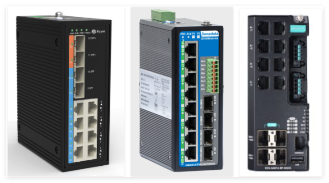
Problem:We once tested a dual power redundant gigabit industrial switch for factory monitoring. This is a rail-mounted industrial switch, and its DDR4 data lines performed normally during prototype testing. However, during small batch trial production, some boards occurred system crashes and data verification problems. Measuring the DDR clock and data lines with an oscilloscope revealed insufficient eye diagram opening and excessive jitter.
Cause Analysis: After inspection by engineers, it was found that this dual power redundant gigabit industrial switch for factory monitoring was designed with a theoretical impedance control of 50Ω for DDR routing,but in actual PCB production, there were deviations in the stacking structure, line width, and dielectric thickness. TDR testing revealed that the impedance of critical data lines dropped to 42Ω at the vias and BGA pads, forming significant discontinuities, leading to signal reflection and eye diagram collapse.
Improvement Plan: we implemented the following steps for effective optimization: first, we optimized the stacking structure and selected materials with more stable dielectric constants; second, we adjusted the line width compensation values to ensure the actual line width after production was close to the design value; third, we added anti-pad around the vias to reduce parasitic capacitance; fourth, we required the PCB manufacturer to provide impedance test strip reports to ensure batch consistency.
2. Case Two: Reflection Leading to Clock Signal Overshoot
Problem: In 2022, we developed an industrial ethernet switch for traffic road surveillance for a client in the South American transportation industry. During mass production, the 25MHz clock signal of this switch experienced severe overshoot on the rising edge, reaching 4.2V (standard 3.3V), which led to damage to the receiving chip.
Cause Analysis: The routing length between the clock source and the receiving end was about 12cm, but the issue was that there was no series matching resistor at the source end, no any parallel matching at the end. When the signal reached the end, total reflection occurred, causing energy accumulation and overshoot.
Improvement Plan: Ultimately, our improvement suggestion was to add a 22Ω or 33Ω resistor in series at the clock source end to match the routing characteristic impedance and absorb reflected energy. But if the board had already been mass-produced and could not be modified, a 100-150Ω resistor could be added in parallel to ground at the end. After modifying the board, the measured overshoot was reduced to below 3.6V, and the chip no longer sustained damage.
3. Case 3: Crosstalk Causes Bit Errors in Adjacent Signal Lines
Problem: For A European automotive parts company's IP40 rugged industrial switch anti-interference, it frequently causes bit errors in the SPI bus when the communication speed is increased to 10MHz, but when the speed is reduced to 5MHz it works well. By measuring with an oscilloscope our engineer found significant crosstalk between the SCK clock line and the MISO data line.
Cause Analysis: Through verification, the length of two signal lines are about 8cm, but the space is only 3mil (twice ofthe line width). And the two signal lines are located on adjacent layers without ground plane isolation. When the rising edge of SCK couples to MISO, it generates a noise spike of about 0.8V, Causing the receiver to misjudge signal levels..
Improvement Plan: After analysis, we implemented several adjustments, including increasing the trace spacing to more than 5 times the line width (at least 12mil); inserting a ground line between the two signal lines; and placing critical signals near the adjacent reference ground plane. After these modifications, after the board modification, crosstalk noise was reduced to below 0.2V, eliminating bit errors and effectively resolving the issue.
4. Systematic Method for Signal Integrity Issues
Through years of practical experience, the technical team at Rayin Technology has developed an effective systematic method, detailed as follows:
Step 1: Simulation Prediction During the PCB design phase, use SI simulation tools (such as HyperLynx, ADS, or Sigrity) to analysis on critical signals. Focus on high-speed interfaces such as clock, DDR, SerDes, USB, and HDMI. By simulation, it can identify potential risks of impedance discontinuity, reflection, and crosstalk, and so engineer can design optimization in advance.
Step 2: TDR Impedance Testing After PCB prototyping, use TDR (Time Domain Reflectometer) to test the actual impedance of critical signal lines. And the test points should include the starting end of the trace, the middle section, the end, at vias, and at BGA pads. If the impedance deviation exceeds ±10%, it require to analyze the cause.
Step 3: Oscilloscope Time Domain Measurement After assembly, use a high-bandwidth oscilloscope (at least 3-5 times the signal frequency) to measure the signal waveform. Engineer should real-time monitor rise time overshoot, ringing, eye diagram, and jitter and compare with design simulation results to confirm consistency.
Step 4: Rectification and Verification After identifying issues, you can rectify them through board modifications, adding matching resistors, adjusting line spacing, etc.,
5. Collaborative Improvement of Design and Production
Overall, the signal integrity issues often require collaboration between the design and production to resolve. The design should provide detailed impedance control requirements and stacking structures; the production should process strictly according to the parameters, and provide test reports.
For more technical cases, you can visit the Rayin Technology official website (www.szrayin.com) to view related articles.